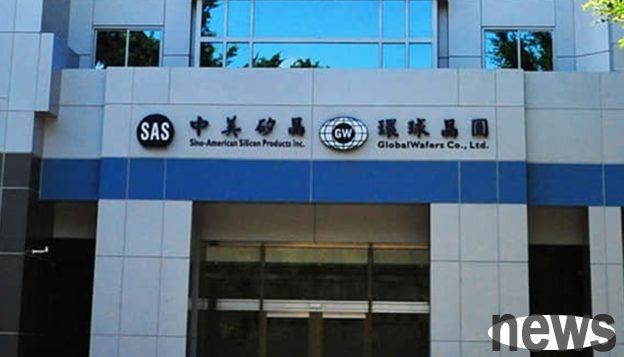
Silicon wafer major Global Wafer held a board of directors meeting on the 4th, during which the financial report for the third quarter ended September 30, 2025 was approved. The consolidated revenue was 14.49 billion yuan, a decrease of 9.46% from the second quarter and a decrease of 8.67% from the same period in 2024. The operating gross profit margin was 18.4%, the operating net profit margin was 8.5%, the after-tax net profit was 1.97 billion yuan, the after-tax net profit rate was 13.6%, and the EPS was 4.12 yuan. Cumulatively, consolidated revenue in the first three quarters of 2025 was 46.1 billion yuan, a decrease of 0.4% from the same period in 2024, operating gross profit margin was 23.6%, operating net profit margin was 13.6%, after-tax net profit was 5.11 billion yuan, after-tax net profit margin was 11.1%, and EPS was 10.68 yuan.
Global Wafer stated that its revenue in the third quarter of 2025 was high due to some customers shipping in advance of the second quarter in order to reduce uncertainty risks, resulting in a quarterly decrease in the short term. Moreover, the exchange rate has fluctuated violently since 2025. The New Taiwan dollar appreciated significantly against the US dollar in the first half of the year, and began to depreciate slowly in August. Since global wafer revenue is mainly in US dollars, exchange rate changes affect the conversion of revenue denominated in New Taiwan dollars, resulting in a relatively flat annual growth rate. If calculated in US dollars, Global Wafer's consolidated revenue in the third quarter was US$490 million, a decrease of 5.95% from the second quarter. Cumulative revenue in the first three quarters reached US$1.48 billion, an increase of 2.45% compared with the same period in 2024. Overall, the difference between the decline in Taiwan dollar-denominated revenue and the growth in US dollar-denominated revenue shows that exchange rate appreciation has had a significant depressive effect on book revenue, and the company's actual operations, which are dominated by US dollars, remain stable.
The global political and economic environment is still volatile, the US tariff policy and the 232 investigation are not yet clear, the visibility of the end market is low, and the overall demand has not yet clearly recovered. The rapid expansion of AI applications has driven demand for high-end logic and memory products. However, the growth momentum is mainly concentrated in the AI field, and the recovery pace of mature process products is relatively slow. In the silicon wafer market, although AI demand has driven up significant growth in overall semiconductor revenue, the recovery rate of wafer shipments has been relatively moderate, mainly because demand for mature process products is still at a low level, and inventory depletion of some terminals continues. Overall, the market has shown a return to a healthy growth path.
On the other hand, tariffs have also significantly increased the demand for local supply from customers around the world, reflecting the importance customers place on supply chain stability and delivery reliability. As major customers accelerate sample delivery and product verification, the U.S. market is expected to become one of the important growth drivers for Global Wafer's mid- to long-term operations. The market inventory adjustment is coming to an end, AI applications continue to penetrate into more industrial fields, and wafer demand is expected to rebound steadily. Global Wafer will continue to strengthen its global layout and local supply through technological upgrades and operational efficiency improvements, and seize the long-term opportunities brought by AI, high-performance computing, and localization to seize industry recovery opportunities and steadily promote long-term growth.
The trend of global localization is accelerating, and Global Wafer's production expansion plans in the United States and Europe are advancing steadily. The Missouri factory in the United States has started trial production in 2025, continues to deliver SOI wafer samples, and will enter mass production in 2026. The new Texas plant (GWA) actively cooperates with customers to verify their products and accelerates the production capacity layout in response to the localization trend in the United States. In the future, it will gradually increase the volume according to market and customer needs. In Europe, the FAB300 plant in Novara, Italy, opened in October. It is one of the few 12-inch semiconductor wafer fabs in Europe with consistent process capabilities. It has now entered the stage of sample delivery and small-volume shipments. This layout not only strengthens the resilience of the European semiconductor supply chain, but also brings Global Wafer closer to customers and supports its long-term development strategy.
The above-mentioned new factory will fully use renewable energy during the mass production phase and comply with the RE100 standard. In addition to demonstrating Global Wafer's commitment to sustainable operations and carbon reduction, it will also help customers increase the proportion of green supply chains and help achieve ESG goals such as RE100 and net-zero emissions. At the same time, Global Wafer has completed a number of production capacity expansion plans in major locations in Asia, continues to optimize process efficiency and supply flexibility, and formed a complementary production capacity network with new factories in Europe and the United States to further enhance the stability of the global supply chain and local service capabilities, and flexibly adjust production capacity allocation to respond to the rapidly changing international economic and trade environment.
In addition, Global Crystal's new material plan is also progressing steadily. The company has completed prototype development of square silicon wafers and 12-inch silicon carbide (SiC) wafers and has entered the sample delivery stage. Square silicon wafers can improve material utilization and packaging design flexibility; silicon carbide wafers have high thermal conductivity and high strength properties, and have development potential for high-power and high-frequency components. At the same time, the company continues to deepen core processes such as cutting, grinding and polishing, gradually strengthens the technological capabilities of new materials, seizes market opportunities in advance, and lays the foundation for the next stage of high-end process demand.
