
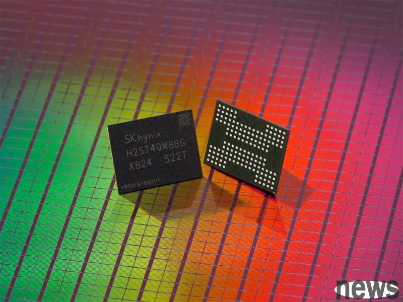
Korean memory manufacturer SK Hynix announced that it has launched 321-layer 2Tb QLC NAND Flash products and started mass production.
SK Hynix said that NAND Flash chips can store information per unit cell (Cell), are divided into different specifications such as SLC (Single level Cell, 1 bit), MLC (Multi Level Cell, 2 bit), TLC (Triple Level Cell, 3 bit), QLC (Quadruple Level Cell, 4 bit), PLC (Penta Level Cell, 5 bit), etc. The larger the information storage capacity of a unit, the more data it can be stored in the single plane.
SK Hynix pointed out that the company was the first in the world to complete the development of more than 300 layers of QLC NAND Flash, once again breaking through the technical limit. The product has the highest degree of integration among existing NAND Flash products. After verification by global customer companies, the project officially entered the AI data center market in the first half of 2026.
SK Hynix emphasized that in order to increase the cost competitiveness of this product by the maximum limit, the company has developed a 2Tb product with doubled capacity compared to existing products. Generally speaking, the larger the capacity of NAND Flash, the more information stored in the unit, and the more complicated the memory management, the slower the data processing speed. To this end, the company has expanded the Plane architecture that can be independently operated within NAND Flash from four planes to six planes, thereby improving and processing capabilities, solving the performance degradation caused by large capacity.
In fact, a plane refers to a single cell and a peripheral circuit that can operate independently in a single wafer. Increased it from 4 to 6, improving simultaneous reading performance with one of the Data Bandwidth. Therefore, the product not only achieves high capacity, but also has a significantly improved performance than previous QLC products. Data transfer speed doubled, writing performance increased by up to 56%, and reading performance increased by 18%. At the same time, data write efficiency has also increased by more than 23%, and it has also gained stronger competitiveness in areas such as AI data centers that require low power consumption.
The company plans to first apply 321-layer NAND Flash on computer-side solid-state drives (PC SSDs), and then gradually expand to enterprise-level solid-state drives (eSSDs) and embedded memory (UFS) products for smart phones. In addition, the company will also officially enter the ultra-high capacity eSSD market for AI servers based on the unique packaging technology stacking 32 NAND Flashes to achieve twice the integration level than the current one.
SK Hynix NAND Flash, deputy president Zheng Yupiao, said that the product started mass production this time, greatly strengthening the high-capacity storage product combination, while ensuring cost competition. In order to meet the rapidly growing AI demand and high performance requirements in the data center market, we will serve as a full-scale memory provider for AI to achieve a larger flight.